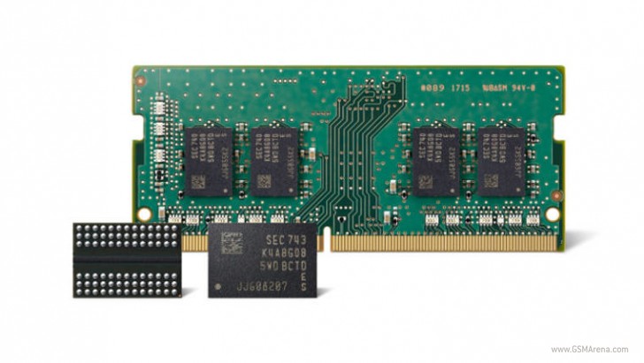
Samsung is now mass-producing the second generation of its
10-nanometer class 8Gb (read gigabit, not gigabyte) DDR4 DRAM, which
will be the foundation for its future DDR4 RAM.
The new generation of 10nm class RAM is about 10% faster and 15% more efficient than the previous one.
 The new 8Gb DD4 can operate at 3,600 megabits per second per pin compared to the 3,200 Mbps of the previous generation.
All of this means that Samsung has a better base on which it will soon begin production of faster RAM to be used in smartphones, laptops, PCs, smartwatches and all sorts of smart devices.
“By developing innovative technologies in DRAM circuit design and process, we have broken through what has been a major barrier for DRAM scalability,” said Gyoyoung Jin, president of Memory Business at Samsung Electronics. “Through a rapid ramp-up of the 2nd-generation 10nm-class DRAM, we will expand our overall 10nm-class DRAM production more aggressively, in order to accommodate strong market demand and continue to strengthen our business competitiveness.”
Samsung’s 2nd-generation 10nm-class 8Gb DDR4 features an approximate 30 percent productivity gain over the company’s 1st–generation 10nm-class 8Gb DDR4. In addition, the new 8Gb DDR4’s performance levels and energy efficiency have been improved about 10 and 15 percent respectively, thanks to the use of an advanced, proprietary circuit design technology. The new 8Gb DDR4 can operate at 3,600 megabits per second (Mbps) per pin, compared to 3,200 Mbps of the company’s 1x-nm 8Gb DDR4.
To enable these achievements, Samsung has applied new technologies, without the use of an EUV process. The innovation here includes use of a high-sensitivity cell data sensing system and a progressive “air spacer” scheme.
In the cells of Samsung’s 2nd-generation 10nm-class DRAM, a newly devised data sensing system enables a more accurate determination of the data stored in each cell, which leads to a significant increase in the level of circuit integration and manufacturing productivity.

The new 10nm-class DRAM also makes use of a unique air spacer that has been placed around its bit lines to dramatically decrease parasitic capacitance**. Use of the air spacer enables not only a higher level of scaling, but also rapid cell operation.
With these advancements, Samsung is now accelerating its plans for much faster introductions of next-generation DRAM chips and systems, including DDR5, HBM3, LPDDR5 and GDDR6, for use in enterprise servers, mobile devices, supercomputers, HPC systems and high-speed graphics cards.
Samsung has finished validating its 2nd-generation 10nm-class DDR4 modules with CPU manufacturers, and next plans to work closely with its global IT customers in the development of more efficient next-generation computing systems.
In addition, the world’s leading DRAM producer expects to not only rapidly increase the production volume of the 2nd-generation 10nm-class DRAM lineups, but also to manufacture more of its mainstream 1st-generation 10nm-class DRAM, which together will meet the growing demands for DRAM in premium electronic systems worldwide.
The new generation of 10nm class RAM is about 10% faster and 15% more efficient than the previous one.
 The new 8Gb DD4 can operate at 3,600 megabits per second per pin compared to the 3,200 Mbps of the previous generation.
All of this means that Samsung has a better base on which it will soon begin production of faster RAM to be used in smartphones, laptops, PCs, smartwatches and all sorts of smart devices.
“By developing innovative technologies in DRAM circuit design and process, we have broken through what has been a major barrier for DRAM scalability,” said Gyoyoung Jin, president of Memory Business at Samsung Electronics. “Through a rapid ramp-up of the 2nd-generation 10nm-class DRAM, we will expand our overall 10nm-class DRAM production more aggressively, in order to accommodate strong market demand and continue to strengthen our business competitiveness.”
Samsung’s 2nd-generation 10nm-class 8Gb DDR4 features an approximate 30 percent productivity gain over the company’s 1st–generation 10nm-class 8Gb DDR4. In addition, the new 8Gb DDR4’s performance levels and energy efficiency have been improved about 10 and 15 percent respectively, thanks to the use of an advanced, proprietary circuit design technology. The new 8Gb DDR4 can operate at 3,600 megabits per second (Mbps) per pin, compared to 3,200 Mbps of the company’s 1x-nm 8Gb DDR4.
To enable these achievements, Samsung has applied new technologies, without the use of an EUV process. The innovation here includes use of a high-sensitivity cell data sensing system and a progressive “air spacer” scheme.
In the cells of Samsung’s 2nd-generation 10nm-class DRAM, a newly devised data sensing system enables a more accurate determination of the data stored in each cell, which leads to a significant increase in the level of circuit integration and manufacturing productivity.

The new 10nm-class DRAM also makes use of a unique air spacer that has been placed around its bit lines to dramatically decrease parasitic capacitance**. Use of the air spacer enables not only a higher level of scaling, but also rapid cell operation.
With these advancements, Samsung is now accelerating its plans for much faster introductions of next-generation DRAM chips and systems, including DDR5, HBM3, LPDDR5 and GDDR6, for use in enterprise servers, mobile devices, supercomputers, HPC systems and high-speed graphics cards.
Samsung has finished validating its 2nd-generation 10nm-class DDR4 modules with CPU manufacturers, and next plans to work closely with its global IT customers in the development of more efficient next-generation computing systems.
In addition, the world’s leading DRAM producer expects to not only rapidly increase the production volume of the 2nd-generation 10nm-class DRAM lineups, but also to manufacture more of its mainstream 1st-generation 10nm-class DRAM, which together will meet the growing demands for DRAM in premium electronic systems worldwide.


No comments:
Post a Comment